WEK35391-2017 Spatial Resolution Test Card,Industrial CT Model
Mode:WEK35391-2017
Type:QA-Phantom
Contact: ken@hkmedqc.com
WEK35391-2017 Spatial Resolution Test Card,Industrial CT Model.PDF

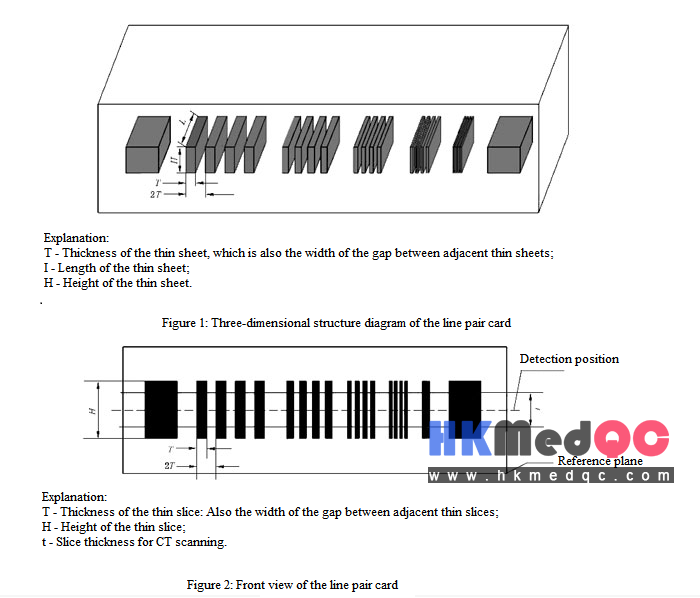
WEK35391-2017 Spatial Resolution Test Card. Each line pair group of the WEK35391-2017 resolution test card is composed of 4 thin plates of the same size arranged parallelly (the plates are separated by metal partitions of the same thickness as the plates). On both sides, calibration blocks with twice the thickness of the thickest plate are placed. The interval between the metal plate groups in each line pair card is 2.5mm.
WEK35391-2017 Spatial Resolution Test Card complies with the requirements of GB/T 35391-2017 Non-destructive testing — Spatial resolution test card for industrial computed tomography (CT) inspection.
The wire pair cards are classified into three types based on their resolution:
1) Grade I Line Pair Card
2) Grade II Line Pair Card
3) Grade III Line Pair Card
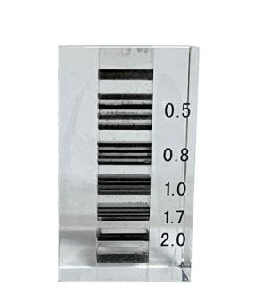
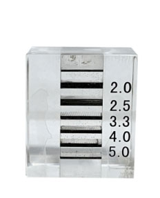
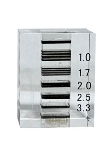
The line pair card is a standard test piece used to test the spatial resolution of industrial CT systems. It is composed of a group of line pairs made of thin sheets of steel, silicon, or other materials agreed upon by the supplier and the buyer. Each line pair group consists of 4 thin sheets of the same size arranged parallelly (the sheets are separated by metal spacers of the same thickness as the sheets), and calibration blocks twice the thickness of the thickest sheet are placed on both sides. Its three-dimensional structure is shown in Figure 1, and the top view is shown in Figure 2.
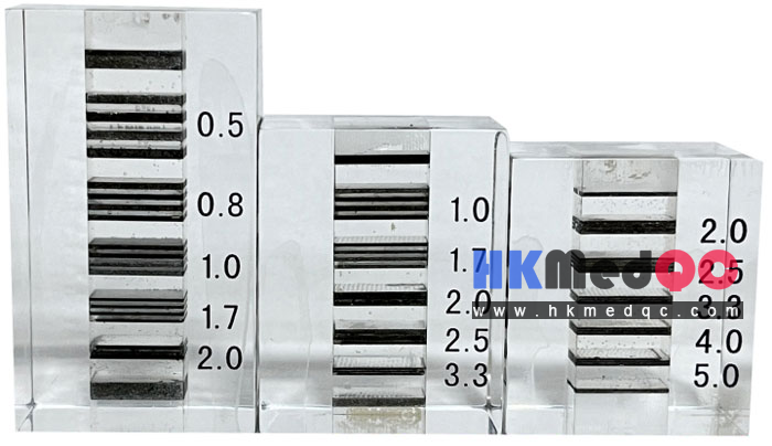
WEK35391-2017 Spatial Resolution Test Card, Photograph of the physical sample of WEK35391-2017 Resolution Test Card:
WEK35391-2017 Spatial Resolution Test Card, Parameters and Specifications of WEK35391-2017 Resolution Test Card:
The thickness of each line pair group of the sheet is T, and the width of the adjacent sheet gap (the thickness of the metal spacer) is also T. The sheet thickness T and the corresponding number of line pairs for various grade line pair cards are shown in Table A.1.
The length L of each strip in the line pair group is 10mm, and the width W is 8mm.
The external dimensions are length (L), width (W), and height (H), with units in mm.
Round hole cards or fine wire cards are divided into two types according to the size of the hole diameter or wire diameter:
1) Grade I round hole card or Grade I fine wire card
2) Grade II round hole card or Grade II fine wire card;
WEK35391-2017 Disk Card
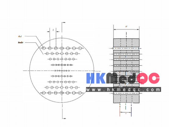
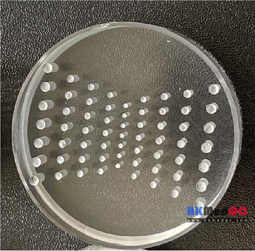
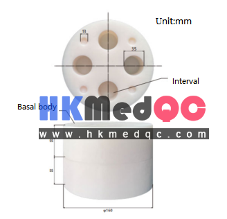
The round hole card is processed on a homogeneous cylindrical base with a series of circular holes of different diameters, and the holes are arranged in rows orderly. The structure is shown in Figure 3. The fine wire card is arranged on a uniform low-density cylindrical base with a series of wires of different diameters, and the wires are arranged in rows orderly.
The disk card is a cylindrical body made of homogeneous rigid material, and its structure is as shown in the following figure. The material of the disk card should be the same as or similar to the radiation absorption characteristics of the object being tested. It is recommended to use steel or silicon (or the material determined by the supplier and the demander).
GBT 35386-2017 Air Gap Test Block
The air gap test block is an artificial air gap of a certain diameter and height manufactured in a homogeneous rigid matrix material [generally steel (e.g. Q235), aluminum (such as 3003), polypropylene], so that the local average density within the slice thickness changes, thereby testing the density resolution. Its basic structure is shown in Figure A.5.
The matrix consists of two high-density cylindrical bodies, with a height of more than 15mm. The diameter of the groove φ is not less than 20mm. The diameter of the cylindrical body can be specified according to the actual situation, generally not less than 3φ. The depth of the groove h is determined according to the slice thickness and the actual situation.
WEK35391-2017 Spatial Resolution Test Card complies with the requirements of GB/T 35391-2017 Non-destructive testing — Spatial resolution test card for industrial computed tomography (CT) inspection.
The wire pair cards are classified into three types based on their resolution:
1) Grade I Line Pair Card
2) Grade II Line Pair Card
3) Grade III Line Pair Card
The line pair card is a standard test piece used to test the spatial resolution of industrial CT systems. It is composed of a group of line pairs made of thin sheets of steel, silicon, or other materials agreed upon by the supplier and the buyer. Each line pair group consists of 4 thin sheets of the same size arranged parallelly (the sheets are separated by metal spacers of the same thickness as the sheets), and calibration blocks twice the thickness of the thickest sheet are placed on both sides. Its three-dimensional structure is shown in Figure 1, and the top view is shown in Figure 2.
WEK35391-2017 Spatial Resolution Test Card, Photograph of the physical sample of WEK35391-2017 Resolution Test Card:
WEK35391-2017 Spatial Resolution Test Card, Parameters and Specifications of WEK35391-2017 Resolution Test Card:
The thickness of each line pair group of the sheet is T, and the width of the adjacent sheet gap (the thickness of the metal spacer) is also T. The sheet thickness T and the corresponding number of line pairs for various grade line pair cards are shown in Table A.1.
| Grade | Group One | Group Two | Group Three | Group Four | Group Five | |||||
| Film thickness T mm |
Demand pairs Lp/mm |
Film thickness T mm |
Demand pairs Lp/mm |
Film thickness T mm |
Demand pairs Lp/mm |
Film thickness T mm |
Demand pairs Lp/mm |
Film thickness T mm |
Demand pairs Lp/mm |
|
| Ⅲ | 0.100 | 5.0 | 4.0 | 4.0 | 0.150 | 3.3 | 0.200 | 2.5 | 0.250 | 2.0 |
| Ⅱ | 0.150 | 3.3 | 2.5 | 2.5 | 0.250 | 2.0 | 0.300 | 1.7 | 0.500 | 1.0 |
| Ⅰ | 0.250 | 2.0 | 1.7 | 1.7 | 0.500 | 1.0 | 0.650 | 0.8 | 1.000 | 0.5 |
The length L of each strip in the line pair group is 10mm, and the width W is 8mm.
The external dimensions are length (L), width (W), and height (H), with units in mm.
| Image |
 |
 |
 |
| Grade | Ⅰ |
Ⅱ |
Ⅲ |
| Line pair |
0.5 to 2.0LP/m |
1.0 to3.3LP/m |
2.0 to5.0LP/m |
| Size (mm) |
45Lx26Wx20H | 33Lx26Wx20H |
30Lx26Wx20H |
Round hole cards or fine wire cards are divided into two types according to the size of the hole diameter or wire diameter:
1) Grade I round hole card or Grade I fine wire card
2) Grade II round hole card or Grade II fine wire card;
WEK35391-2017 Disk Card
The round hole card is processed on a homogeneous cylindrical base with a series of circular holes of different diameters, and the holes are arranged in rows orderly. The structure is shown in Figure 3. The fine wire card is arranged on a uniform low-density cylindrical base with a series of wires of different diameters, and the wires are arranged in rows orderly.
The disk card is a cylindrical body made of homogeneous rigid material, and its structure is as shown in the following figure. The material of the disk card should be the same as or similar to the radiation absorption characteristics of the object being tested. It is recommended to use steel or silicon (or the material determined by the supplier and the demander).
GBT 35386-2017 Air Gap Test Block
The air gap test block is an artificial air gap of a certain diameter and height manufactured in a homogeneous rigid matrix material [generally steel (e.g. Q235), aluminum (such as 3003), polypropylene], so that the local average density within the slice thickness changes, thereby testing the density resolution. Its basic structure is shown in Figure A.5.
The matrix consists of two high-density cylindrical bodies, with a height of more than 15mm. The diameter of the groove φ is not less than 20mm. The diameter of the cylindrical body can be specified according to the actual situation, generally not less than 3φ. The depth of the groove h is determined according to the slice thickness and the actual situation.
SAG: WEK35391-2017,WEK35391-2017 Resolution Test Card,Spatial Resolution Test Card,39391 Spatial Resolution Test Card,Industrial CT Resolution Test Card